Table of Contents
What is P-N Junction?
When a p-type semiconductor is brought in close contact with an n-type semiconductor, the resulting arrangement is called P-N Junction. P-N junction is also called Junction diode.
Formation of P-N Junction:
First of all, grow p-type semi-conductor by adding impurities from group III of the periodic table to Si or Ge. But before the process is completed, start growing n-type semiconductor by adding impurities from group V of the periodic table to Si or Ge. Thus, the crystal obtained is one single whole, one half of which functions as p-type and the other half of which functions as n-type. There is a well-defined junction between the two portions.
Potential Barrier:
Due to the difference in concentration between electrons and holes in the two regions of the P-N junction, the electrons from the n-region diffuse through the junction into the p-region and holes from the p-region diffuse into the n-region.
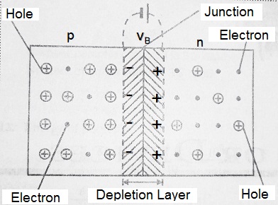
The accumulation of electric charges of opposite polarities in the two regions of the junction gives rise to an electric field. This is as if a fictitious battery is connected across the junction. This electric field opposes the further flow of electrons from the n-region to the p-region and also opposes the flow of holes from the p-region to the n-region. Hence, this electric field sets a potential barrier VB at the junction. This potential barrier opposes further diffusion of electrons and holes in opposite regions. The Potential barrier for Ge is 0.3 volts and for Si is 0.7 volts.
Depletion Layer:
A thin layer on both sides of Junction J, which carries no charge is called the Depletion layer.
Symbolic Representation:
A p-n junction is represented symbolically as shown in figure-

Working or Biasing of P-N Junction:
There are two types of Biasing-
Forward Biasing:
A p-n junction is said to be forward-biased if the positive terminal of external battery ‘B’ is connected to p-side and the negative terminal of the battery ‘B’ is connected to n-side of the p-n junction.
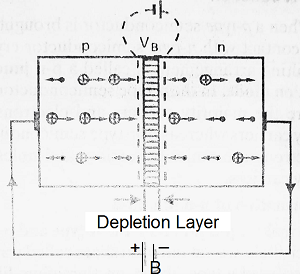
If the voltage applied by the battery is greater than VB, then the holes in the p-region will cross the potential barrier and enter the n-region and the electrons will also cross the potential barrier and reach the p-region. Hence electrons and holes, both start flowing in opposite directions and hence they constitute the flow of current in the semiconductor. In this forwarded biasing, both the potential barrier and depletion layer are reduced. We can also say, the p-n junction offers low resistance to the flow of current in the case of forward biasing.
Reverse Biasing:
A p-n junction is said to be reverse-biased if the positive terminal of external battery ‘B’ is connected to n-side and the negative terminal of the battery is connected to p-side of the p-n junction.
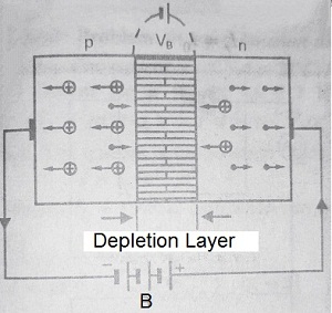
In this case, the majority carriers in the two regions are pulled away from the junction and hence there is no flow of majority carriers across the junction. Hence no forwarded current flows through the junction when it is reverse-biased. In this case, both the potential barrier and depletion layer becomes thick. We can also say in reverse biasing, the p-n junction offers high resistance to the forward current.
However, a few minority carriers (holes in the n-region and electrons in the p-region) cross the junction. Hence they constitute the current that flows in opposite direction. This current is called the reverse current or leakage current.



Comments (No)