Table of Contents
Extrinsic Semiconductor:
Definition- A semi-conductor with suitable impurity atoms added to it, is called an extrinsic semiconductor. It is of two types-
- N-Type Semiconductor.
- P-Type Semiconductor.
N-Type Semiconductor:
When atoms from Group V of the periodic table (example- As, P etc.) are added to a pure semiconductor, we get an N-type semiconductor.
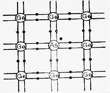
The group V, atoms like As, P, etc. have 5 valence electrons. Out of these five valence electrons, four are shared with the electrons of adjoining Si atoms to form four covalent bonds whereas the fifth electron remains unshared. Thus each Impurity atom added donates one free electron to the crystal structure. These impurity atoms are therefore also called donor atoms.
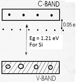
The fifth electron, being unshared, is loosely bound and can easily be liberated from the atom with a very little amount of energy ≅ 0.05 eV. For this reason, the fifth electron of each atom of impurity is shown by 0.05 eV below the conduction band.
At room temperature, some of the covalent bonds may break away and we have free electrons and these electrons move from the valence band to the conduction band. Again holes are created in place of valence electrons in the valence band.
Clearly, in this type of semiconductor, the total number of free electrons far exceeds the total number of holes i.e. ne > nh.
Where ne = number density of electrons in C-Band.
nh = number density of holes in V-Band.
It should be noted that, in N-type semiconductor, the majority carriers are electrons and the minority carriers are holes.
P-Type Semiconductor:
When atoms from group III of the periodic table (example- B, Al, etc.) are added to a pure semiconductor, we get a P-type semiconductor.
The group III atoms like Boron, Aluminium etc. have three valence electrons. Suppose Boron is added to Silicon. The three valence electrons of Boron make three covalent bonds by sharing the electrons of adjoining silicon atoms. However, the fourth covalent bond remains incomplete, since there is an electron deficiency. This deficiency is completed by taking an electron from one Si-Si bond. Hence a hole is created in the Si-Si bond as shown in the figure. Since these impurity atoms accept the electrons, therefore these impurity atoms are called Acceptor atoms.
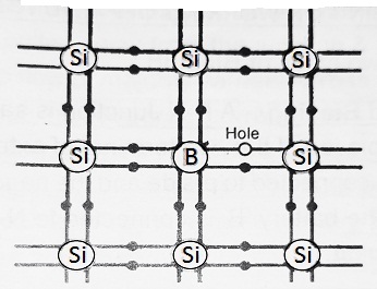
It should be noted that an electron from the Si-Si bond goes to the Boron atom, only if this electron gains additional energy of ≅ 0.01 eV. For this reason, the Holes are shown 0.01 eV above the Valence band.
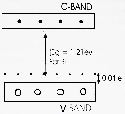
At room temperature, some of the covalent bonds may break away and we have free electrons. These free electrons move from valence band to conduction band, under the application of an external electric field.
Clearly, in this type of semiconductor, the total number of holes far exceeds the total number of electrons i.e. nh > ne.
Where nh, ne is the number density of holes and electrons. It should be noted that, in P-type semiconductor, the majority carriers are holes and the minority carriers are electrons.





Comments (No)